

EN


Project Backgroud
This project focuses on the automation upgrade of the back‑end packaging and testing processes for NAND Flash memory chips, with the development and application of a NAND Flash automatic loading/unloading and sorting machine. The solution assists semiconductor companies in improving production efficiency, ensuring product quality, and reducing operational costs, while promoting the intelligent and scalable development of the memory chip packaging and testing segment.
The current manufacturing processes are primarily confronted with the following challenges:
✅ Low efficiency in manual operations, making it difficult to meet capacity expansion needs.
✅ Insufficient sorting accuracy.
✅ High labour costs.
✅ Significant human‑induced errors.
The equipment developed in this project is positioned as a domestic alternative, integrating core technologies such as vision positioning, servo drive, and intelligent control. It is compatible with mainstream NAND Flash chip specifications in China, accommodates multiple package types and testing standards, and can flexibly interface with factory MES systems for real‑time production data traceability and intelligent scheduling. This provides semiconductor packaging and testing enterprises with a cost‑effective, highly flexible, and reliable automated solution, enabling them to enhance market competitiveness and driving the self‑reliant development of the domestic memory chip industry.
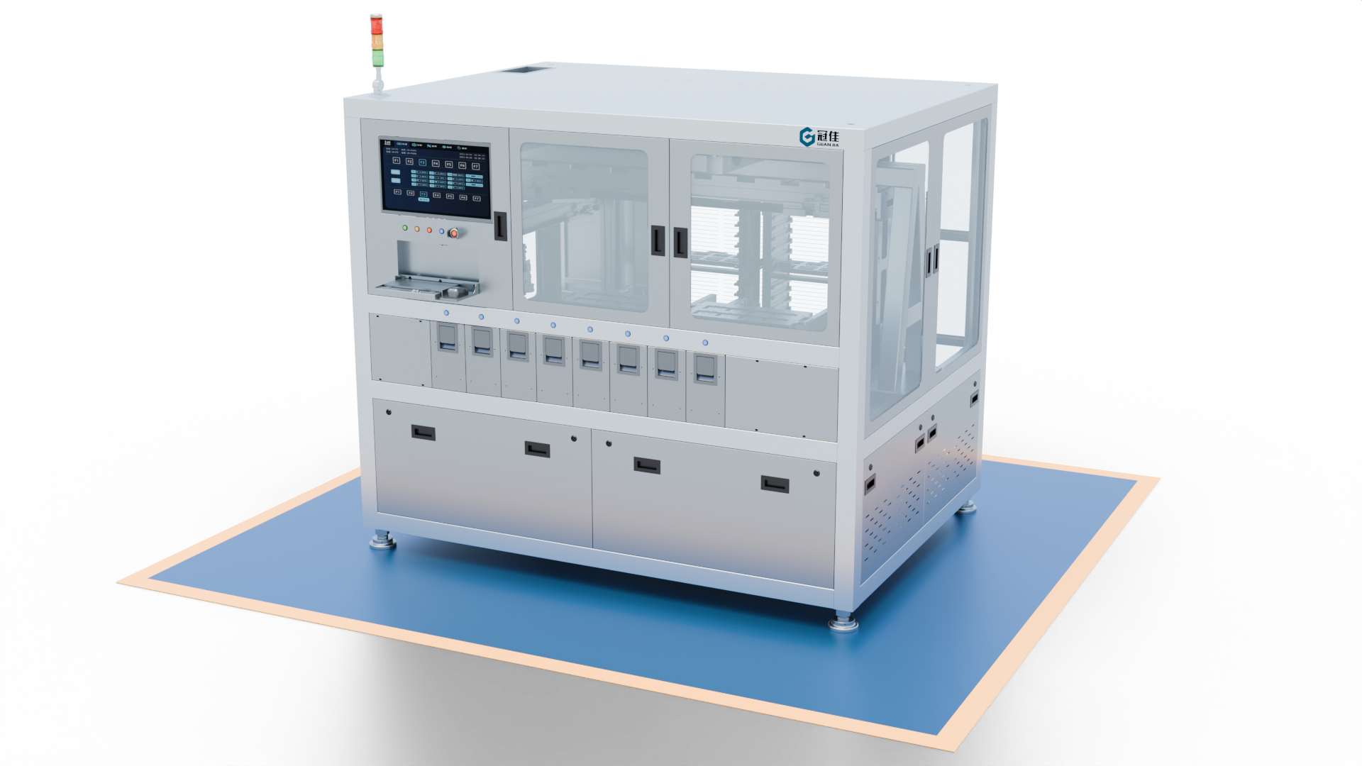
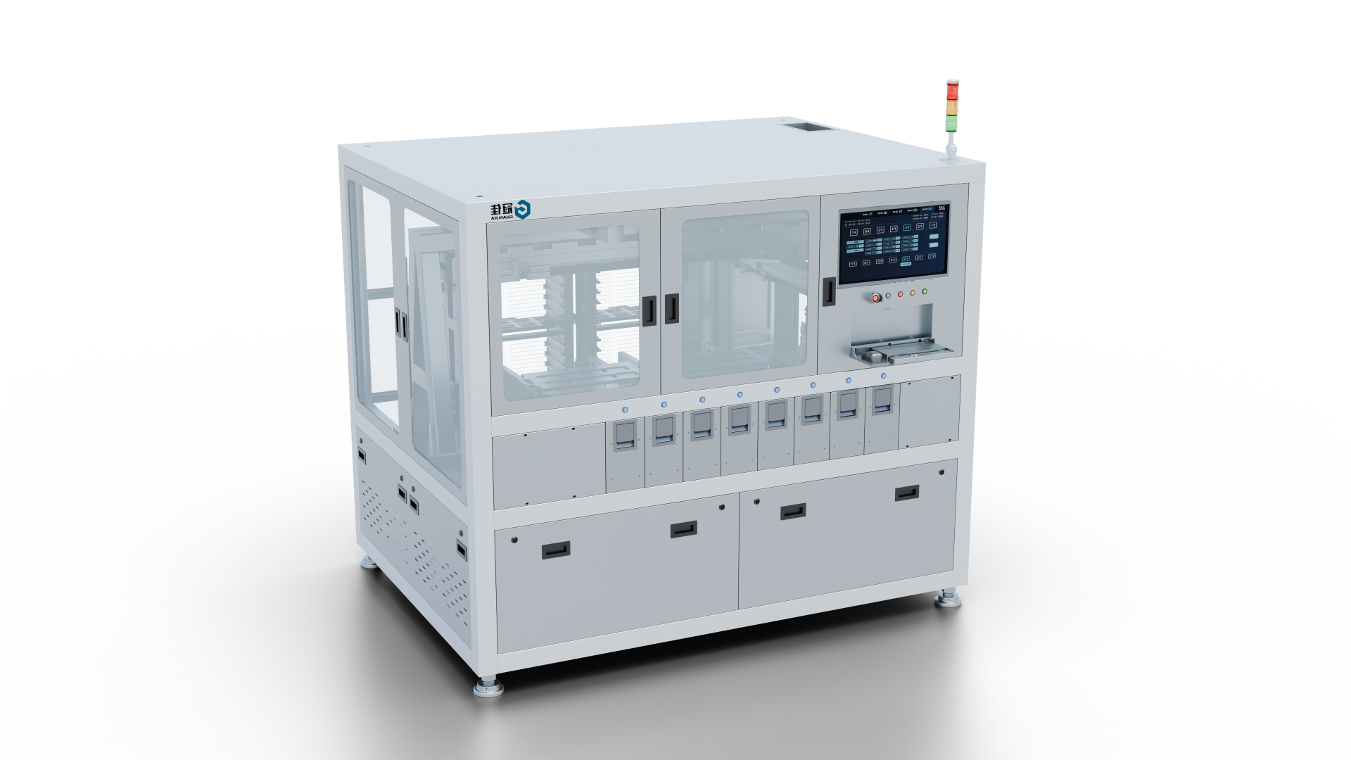
First、Equipment Overview and Core Capabilities
The NAND Flash automatic loading/unloading and sorting machine is a core automation equipment in the semiconductor back‑end packaging and testing field. It is specifically designed for automatic loading/unloading, precise transfer, test result capture, and bin sorting of NAND Flash chips (including derived memory chips such as eMMC, UFS, and DRAM) before and after burn‑in testing and electrical performance testing. The system supports bidirectional conversion between trays and burn‑in boards (BIBs), making it a critical piece of equipment for achieving scalable and standardised memory chip production.
Second、Equipment Specifications and Parameters
1.Dimensions:2.3m (L) × 1.7m (W) × 2.0m (H).
2.Transfer Module:Utilises a servo motor with lead screw/synchronous belt drive architecture, paired with quick‑release vacuum nozzles to achieve smooth chip pick‑up and transfer. Select models are equipped with multiple nozzle sets, enabling simultaneous pick‑and‑place of multiple chips for enhanced throughput.
3.Sorting Module:Equipped with up to 8 sorting bins, supporting multi‑criteria bin classification including OK/NG/retest/special acceptance. Chips are automatically sorted into corresponding trays or tubes based on test results. The system incorporates anti‑stacking detection mechanisms (CCD vision inspection and real‑time nozzle monitoring) to ensure sorting accuracy, with high binning precision and zero risk of material mixing.
4.Intelligent Management and Control:Supports real‑time production data traceability, remote monitoring, and centralised intelligent scheduling, enabling smart management of production processes and meeting the requirements of modern manufacturing facilities.

The NAND Flash automatic loading/unloading and sorting machine is primarily applied in the semiconductor back‑end packaging and testing segment, focusing on the automated testing and sorting of NAND Flash memory chips. It is suitable for memory chip manufacturers, packaging and testing enterprises, and serves a wide range of fields including consumer electronics, industrial control, the Internet of Things (IoT), and automotive electronics. The specific application scenarios are as follows:
(一)NAND Flash Chip Packaging and Testing Enterprises
(二)Consumer Electronics Storage Product Manufacturers
(三)Industrial Control and IoT Applications
(四)Automotive Electronics
(五)R&D and Laboratory Settings
(六)High‑Volume Memory Chip Production Lines

 Consultation
